LTC4350
4350fb
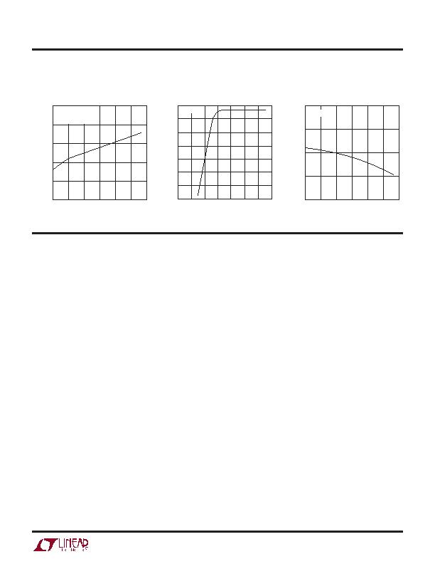
Typical perForMance characTerisTics
Gain Pin Voltage vs Temperature
V
GATE
vs V
CC
V
GATE
vs Temperature
pin FuncTions
UV (Pin 1): Undervoltage Pin. The threshold is set at 1.244V
with a 24mV hysteresis. When the UV pin is pulled high,
the charge pump ramps the GATE pin. When the UV pin
is pulled low, the GATE pin will be pulled low.
OV (Pin 2): Overvoltage Pin. The threshold is set at 1.220V
with a 15mV hysteresis. When the OV pin is pulled high,
the GATE pin is pulled low. After a timer cycle, the STATUS
pin is pulled low until the OV pin is pulled low.
TIMER (Pin 3): Analog System Timing Generator Pin.
This pin is used to set the delay before the load sharing
turns on after the UV pin goes high. The other use for
the TIMER pin is to delay the indication of a fault on the
STATUS pin.
When the timer is off, an internal N-channel shorts the
TIMER pin to ground. When the timer is turned on, a 2礎
or 6礎 timer current (I
TIMER
) from V
CC
is connected to the
TIMER pin and the voltage starts to ramp up with a slope
given by: dV/dt = I
TIMER
/C
T
. When the voltage reaches the
trip point (1.220V), the timer will be reset by pulling the
TIMER pin back to ground. The timer period is given by:
(1.220V " C
T
)/I
TIMER
.
GAIN (Pin 4): Analog Output Pin. The voltage across the
R
+
and R
pins is divided by a 1k resistor and sourced as
a current from the GAIN pin. An external resistor on the
GAIN pin determines the voltage gain from the current
sense resistor to the GAIN pin.
COMP2 (Pin 5): Analog Output Pin. This pin is the output
of the share bus error amplifier E/A2. (A compensation
capacitor between this pin and ground sets the crossover
frequency for the power supply adjustment loop.) In most
cases, this pin operates between 0.5V to 1.5V and repre-
sents a diode voltage up from the voltage at the R
SET
pin.
It is clamped at 3V . During start-up, this pin is clamped to
ground. After a timer cycle (and if the GATE pin is high),
the COMP2 pin is released.
COMP1 (Pin 6): Analog Output Pin. This pin is the output
of the voltage regulating error amplifier E/A1. A com-
pensation capacitor between this pin and ground sets
the crossover frequency of the share bus loop. This pin
operates a diode voltage up from the voltage at the SB
pin and is clamped at 8.4V .
SB (Pin 7): Analog Output Pin. This pin drives the share
bus used to communicate the value of shared load current
between several power supplies. There is an amplifier that
drives this pin a diode below the COMP1 pin using an internal
NPN as a pull-up and a 20k resistor as a pull-down.
TEMPERATURE (癈)
50
2.2
2.3
2.4
2.5
2.6
2.7
25
0
25
50
75
100
R
GAIN
= 25k
(V
R
+
V
R
) = 100mV
V
CC
= 5V
V
CC
(V)
0
10
11
13
6
10
9
8
2
4
8
12 14
7
6
12
T
A
= 25癈
TEMPERATURE (癈)
50
11.0
11.5
12.0
12.5
13.0
25
0
25
50
75
100
V
CC
= 5V
发布紧急采购,3分钟左右您将得到回复。
相关PDF资料
MAX1299CEAE+
IC TEMP SENS W/ADC 16-SSOP
MAX14544ETA+T
IC ACCY SWITCH OVP PROTECT 8TDFN
MAX1617AMEE+T
IC REMOTE/LOCAL TEMP SNSR 16QSOP
MAX1617MEE+T
IC REMOTE/LOCAL TEMP SNSR 16QSOP
MAX1619MEE+
IC TEMP SENSOR W/ALARM 16-QSOP
MAX1765EUE+
IC REG DL BST/LINEAR 16TSSOP
MAX1989MUE+
IC TEMP SENSOR REMOTE 16TSSOP
MAX31723MUA+
IC THERMOMETER/STAT SPI-3W 8UMAX
相关代理商/技术参数
LTC4350IGN#TR
功能描述:IC CNTRLR HOTSWAP LOADSHAR16SSOP RoHS:否 类别:集成电路 (IC) >> PMIC - 热交换 系列:- 产品培训模块:Lead (SnPb) Finish for COTS
Obsolescence Mitigation Program 标准包装:119 系列:- 类型:热交换控制器 应用:通用型,PCI Express? 内部开关:无 电流限制:- 电源电压:3.3V,12V 工作温度:-40°C ~ 85°C 安装类型:表面贴装 封装/外壳:80-TQFP 供应商设备封装:80-TQFP(12x12) 包装:托盘 产品目录页面:1423 (CN2011-ZH PDF)
LTC4350IGN#TRPBF
功能描述:IC CNTRLR HOTSWAP LOADSHAR16SSOP RoHS:是 类别:集成电路 (IC) >> PMIC - 热交换 系列:- 产品培训模块:Lead (SnPb) Finish for COTS
Obsolescence Mitigation Program 标准包装:119 系列:- 类型:热交换控制器 应用:通用型,PCI Express? 内部开关:无 电流限制:- 电源电压:3.3V,12V 工作温度:-40°C ~ 85°C 安装类型:表面贴装 封装/外壳:80-TQFP 供应商设备封装:80-TQFP(12x12) 包装:托盘 产品目录页面:1423 (CN2011-ZH PDF)
LTC4352CDD#PBF
功能描述:IC IDEAL DIODE CNTRL 12-DFN RoHS:是 类别:集成电路 (IC) >> PMIC - O 圈控制器 系列:- 标准包装:1,000 系列:- 应用:电池备份,工业/汽车,大电流开关 FET 型:- 输出数:5 内部开关:是 延迟时间 - 开启:100ns 延迟时间 - 关闭:- 电源电压:3 V ~ 5.5 V 电流 - 电源:250µA 工作温度:0°C ~ 70°C 安装类型:表面贴装 封装/外壳:16-SOIC(0.154",3.90mm 宽) 供应商设备封装:16-SOIC N 包装:带卷 (TR)
LTC4352CDD#TRPBF
功能描述:IC IDEAL DIODE CNTRL 12-DFN RoHS:是 类别:集成电路 (IC) >> PMIC - O 圈控制器 系列:- 标准包装:1,000 系列:- 应用:电池备份,工业/汽车,大电流开关 FET 型:- 输出数:5 内部开关:是 延迟时间 - 开启:100ns 延迟时间 - 关闭:- 电源电压:3 V ~ 5.5 V 电流 - 电源:250µA 工作温度:0°C ~ 70°C 安装类型:表面贴装 封装/外壳:16-SOIC(0.154",3.90mm 宽) 供应商设备封装:16-SOIC N 包装:带卷 (TR)
LTC4352CMS#PBF
功能描述:IC IDEAL DIODE CNTRL 12-MSOP RoHS:是 类别:集成电路 (IC) >> PMIC - O 圈控制器 系列:- 标准包装:1,000 系列:- 应用:电池备份,工业/汽车,大电流开关 FET 型:- 输出数:5 内部开关:是 延迟时间 - 开启:100ns 延迟时间 - 关闭:- 电源电压:3 V ~ 5.5 V 电流 - 电源:250µA 工作温度:0°C ~ 70°C 安装类型:表面贴装 封装/外壳:16-SOIC(0.154",3.90mm 宽) 供应商设备封装:16-SOIC N 包装:带卷 (TR)
LTC4352CMS#TRPBF
功能描述:IC IDEAL DIODE CNTRL 12-MSOP RoHS:是 类别:集成电路 (IC) >> PMIC - O 圈控制器 系列:- 标准包装:1,000 系列:- 应用:电池备份,工业/汽车,大电流开关 FET 型:- 输出数:5 内部开关:是 延迟时间 - 开启:100ns 延迟时间 - 关闭:- 电源电压:3 V ~ 5.5 V 电流 - 电源:250µA 工作温度:0°C ~ 70°C 安装类型:表面贴装 封装/外壳:16-SOIC(0.154",3.90mm 宽) 供应商设备封装:16-SOIC N 包装:带卷 (TR)
LTC4352HDD#PBF
功能描述:IC IDEAL DIODE CTLR W/MON 12-DFN RoHS:是 类别:集成电路 (IC) >> PMIC - O 圈控制器 系列:- 标准包装:1,000 系列:- 应用:电池备份,工业/汽车,大电流开关 FET 型:- 输出数:5 内部开关:是 延迟时间 - 开启:100ns 延迟时间 - 关闭:- 电源电压:3 V ~ 5.5 V 电流 - 电源:250µA 工作温度:0°C ~ 70°C 安装类型:表面贴装 封装/外壳:16-SOIC(0.154",3.90mm 宽) 供应商设备封装:16-SOIC N 包装:带卷 (TR)
LTC4352HDD#TRPBF
功能描述:IC IDEAL DIODE CTLR W/MON 12-DFN RoHS:是 类别:集成电路 (IC) >> PMIC - O 圈控制器 系列:- 标准包装:1,000 系列:- 应用:电池备份,工业/汽车,大电流开关 FET 型:- 输出数:5 内部开关:是 延迟时间 - 开启:100ns 延迟时间 - 关闭:- 电源电压:3 V ~ 5.5 V 电流 - 电源:250µA 工作温度:0°C ~ 70°C 安装类型:表面贴装 封装/外壳:16-SOIC(0.154",3.90mm 宽) 供应商设备封装:16-SOIC N 包装:带卷 (TR)